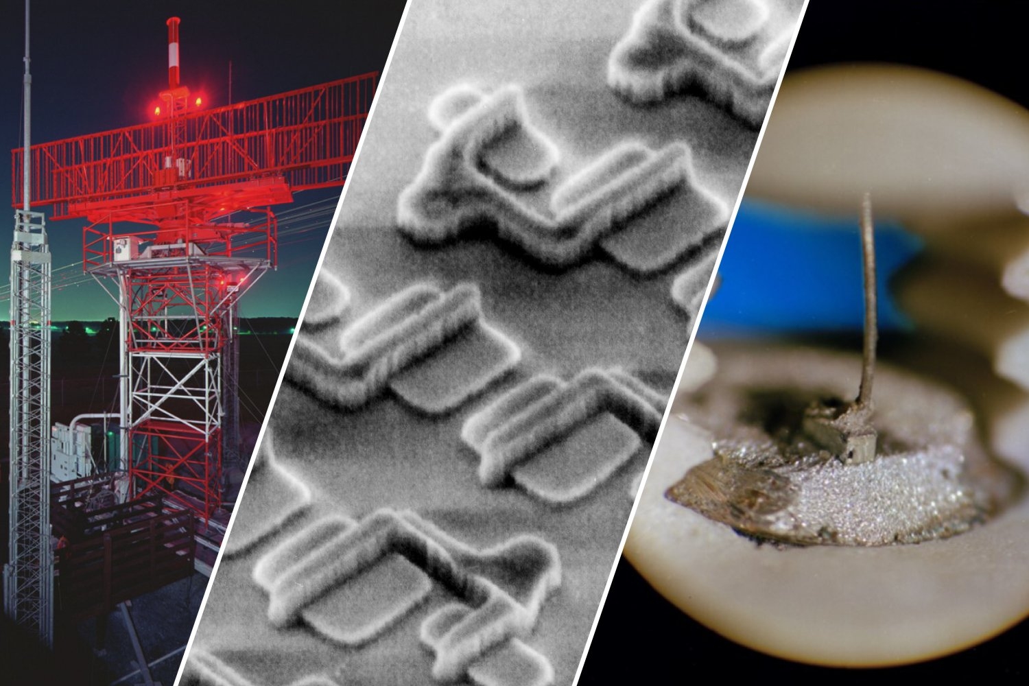
The Institute of Electrical and Electronics Engineers (IEEE) has designated three historic technologies from MIT Lincoln Laboratory as IEEE Milestones. These technologies include Mode S air traffic control (ATC) radar beacon systems, 193 nanometer (nm) lithography and semiconductor lasers. Lincoln Laboratory, General Electric and IBM agree.
As the world’s largest technical professional organization, IEEE’s mission is to “advance technology to benefit mankind.” The Milestone program commemorates innovations developed at least 25 years ago that have achieved this goal.
All three technologies are an integral part of daily life. Anyone who has flown on a commercial aircraft has benefited from Mode S, the system used by air traffic controllers to track aircraft. The integrated circuits that power modern computing and communications devices are fabricated using 193 nm lithography. Perhaps the most ubiquitous are semiconductor lasers—micron-sized light-emitting devices that make possible high-speed Internet and many other technologies that underpin today’s information society.
“MIT Lincoln Laboratory has been a leader in promoting innovations previously thought possible only in science fiction. The three IEEE milestones presented demonstrate these achievements and celebrate the creation of these game-changing technical ingenuity and diversity of teamwork,” said Karen Panetta, vice president of the IEEE Boston Chapter, which presented the award to Lincoln Laboratory at a ceremony on February 2.
Lincoln Laboratory has three IEEE milestones: pioneering the use of packet networks for voice communications, developing the United States’ first air defense system, and collaborating with MIT to create the Whirlwind high-speed digital computer.
Tracking aircraft worldwide
The Mode S ATC radar beacon system was developed to address the challenges of existing ATC beacon radar systems in use in the late 1960s. Commercial air traffic is growing rapidly, causing interference between beacon replies and air traffic control ground radar interrogations. This interference could disrupt aircraft surveillance in high-density airspace.
Lincoln Laboratory, under the auspices of the Federal Aviation Administration (FAA), is leading the development of the technology needed to address this safety issue. Mode S’s advanced communications architecture allows the radar to select specific aircraft for interrogation. To selectively communicate, the system design included modified aircraft transponders, each assigned a unique address code. Upgrades to the radar antenna and signal processing also allow Mode S to accurately determine aircraft position while requiring far fewer air-to-ground messages than previous systems. Mode S also offers a data link feature that enables other critical safety systems such as traffic alert and collision avoidance systems.
Today, Mode S is the global industry standard. An estimated 100,000 aircraft are equipped with Mode S transponders, and more than 900 Mode S radars are deployed worldwide. The technology is also the basis for the FAA’s latest air traffic control surveillance system, which enables continuous flight tracking independent of ground-based radar by using position and speed information broadcast by aircraft.
“This technology affects every flyer on every flight, and Mode S will It was the department that came up with it.” “Without Mode S, we would have a very different air transportation system today, one that would be far less efficient and less safe.”
Powering the microelectronics industry
Over the past 20 years, 193 nm projection lithography has been able to make every chip in every laptop, smartphone, military system and data center.
Photolithography uses light to print tiny patterns onto silicon chips. The patterns are projected onto silicon wafers that are coated with a chemical that changes its solubility when exposed to light. The soluble parts are etched away, leaving behind tiny structures that become the transistors and other devices on the chip.
Shorter wavelengths of light enable printing of smaller features, allowing for denser chip packaging. By the 1980s, the accepted view in the industry was that 248 nm was the shortest wavelength possible for photolithography.
Despite widespread skepticism and technical obstacles, Lincoln Laboratory pioneered 193 nm wavelength lithography, using the technology to create the world’s first microelectronic devices. In 1993, the laboratory installed its first 193 nm projection system. Soon after, the lab opened its doors to industrial partners to guide 193 nm semiconductor manufacturing, paving the way for its widespread adoption. Today, it has become a mainstream technology in the industry and makes integrated circuits increasingly powerful.
“193 nm lithography enables the microelectronics industry to continue on the path to miniaturization in line with Moore’s Law, impacting every aspect of our increasingly digital lives. This is also the result of close collaboration between Lincoln Laboratory and industrial partners A typical example.” said Mordechai Rothschild, one of the main developers of 193 nm technology and now a key staff member in the advanced technology department.
Lighting up the world of new technologies
In the fall of 1962, General Electric, IBM, and Lincoln Laboratory independently reported the first demonstrations of semiconductor lasers. In the 62 years since, it has become the world’s most widely used laser and a fundamental component of numerous technologies: DVDs, CDs, computer mice, laser pointers, barcode scanners, medical imagers, printers, and more. However, its greatest impact is arguably on communications. Every second, semiconductor lasers encode information onto light, which is transmitted across oceans via fiber-optic cables to many homes, forming the backbone of the Internet.
Although the laser was invented a few years ago in 1960, the semiconductor type laser is special because it implements all the laser elements – light generation and amplification, lenses and mirrors – in a piece of semiconductor material no larger than a grain of meter . When an electric current is injected, the material is very efficient at converting electrical energy into light energy. These properties have captured the imagination of scientists and engineers around the world.
“I’m pretty sure that without the low cost and manufacturability of semiconductor lasers, we wouldn’t be streaming movies at home or searching for the best restaurants on our phones,” said Paul Juodawlkis, an expert in photonic devices and integrated circuits and the lab. Head of the Quantum Information and Integrated Nanosystems Group. “It’s great to know that Lincoln Laboratory has played an important role in advancing this technology for government and commercial applications over the past 60-plus years and is prepared to continue to do so in the future.”
Respect inventors and their legacies
Kathleen Kramer, 2024 IEEE President-elect, presented the three awards to Lincoln Laboratory Director Eric Evans during the dedication ceremony. The ceremony took place in the auditorium at Lincoln Laboratory in Lexington, Massachusetts. Evans took the stage with the inventor or his descendant to accept each plaque. Many Lincoln Laboratory staff and retirees who contributed to these innovations were also in attendance.
Vincent Orlando, who spent 50 years of his career in the laboratory developing Mode S technology, accepted the award along with Evans. Mordechai Rothschild and David Shaver unveil 193 nm photolithographic plaques. Both are key developers of the technology.
For some, the ceremony is a touching celebration of their parents’ legacy and a return to fond memories. Richard Rediker, son of semiconductor laser inventor Robert Rediker, recalled his last visit to Lincoln Laboratory more than 60 years ago when he was a child experimenting with his father Play in the room. He accepted the semiconductor medal along with Susan Zeiger and Robert Lax, the children of co-inventors Herbert Zeiger and Benjamin Lax.
“It was so rewarding to meet other children of my father’s colleagues and fully understand the significance of our father’s invention to today’s society. Although my father passed away five years ago, this ceremony brought him back to life for an afternoon.” Redick said, adding that it was an experience he’ll never forget.
Likewise, these technologies have left an indelible mark on the world.
“By celebrating the pride and prestige of our profession’s historical contributions, we demonstrate how engineers, scientists and technical experts contribute not only to our local communities, but to our global community,” Kramer said before presenting the plaque. .” “I am delighted to have known these seminal events and the people behind them. They are milestones in the progress of technology and civilization.”