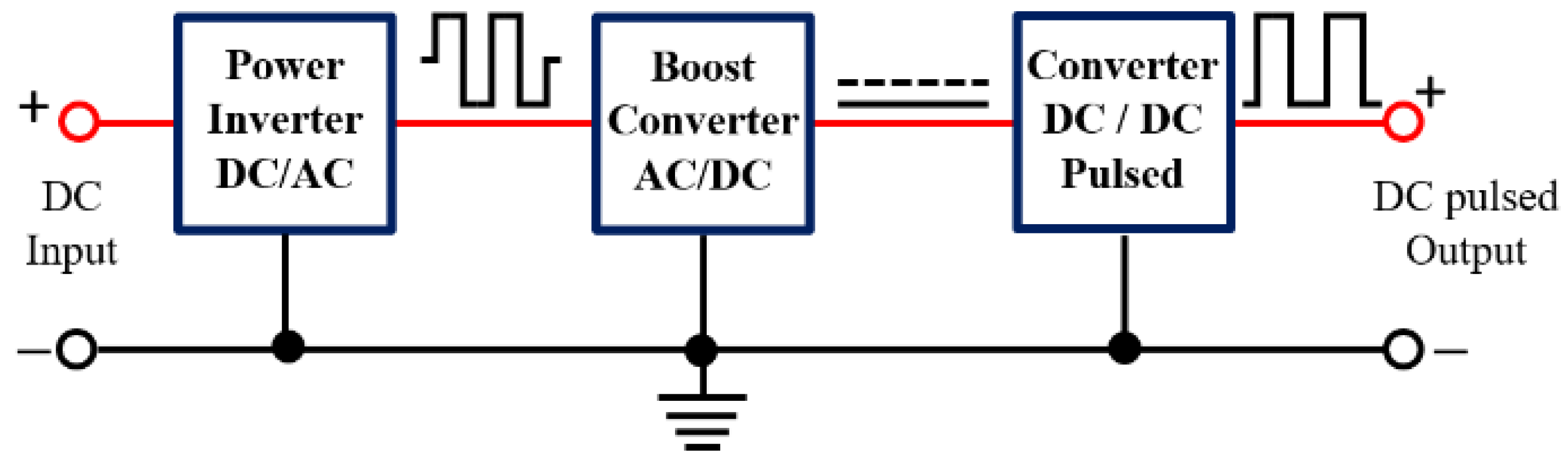
figure 1.
Various stages of pulsed HVDC power supply.
figure 1.
Various stages of pulsed HVDC power supply.
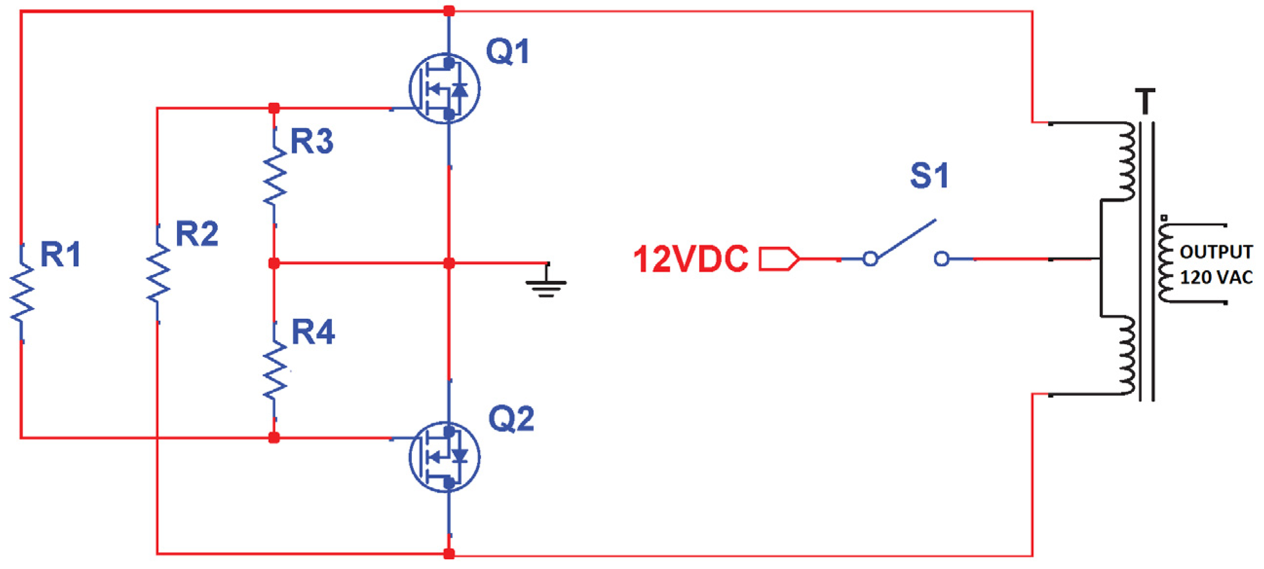
Voltage inverter stage circuit design [30].
Voltage inverter stage circuit design [30].
Full-wave Greinacher voltage four-way circuit [31]. (A) Positive half cycle, (Second) negative half cycle.
Full wave Greinacher voltage four-way circuit [31]. (A) Positive half cycle, (Second) negative half cycle.
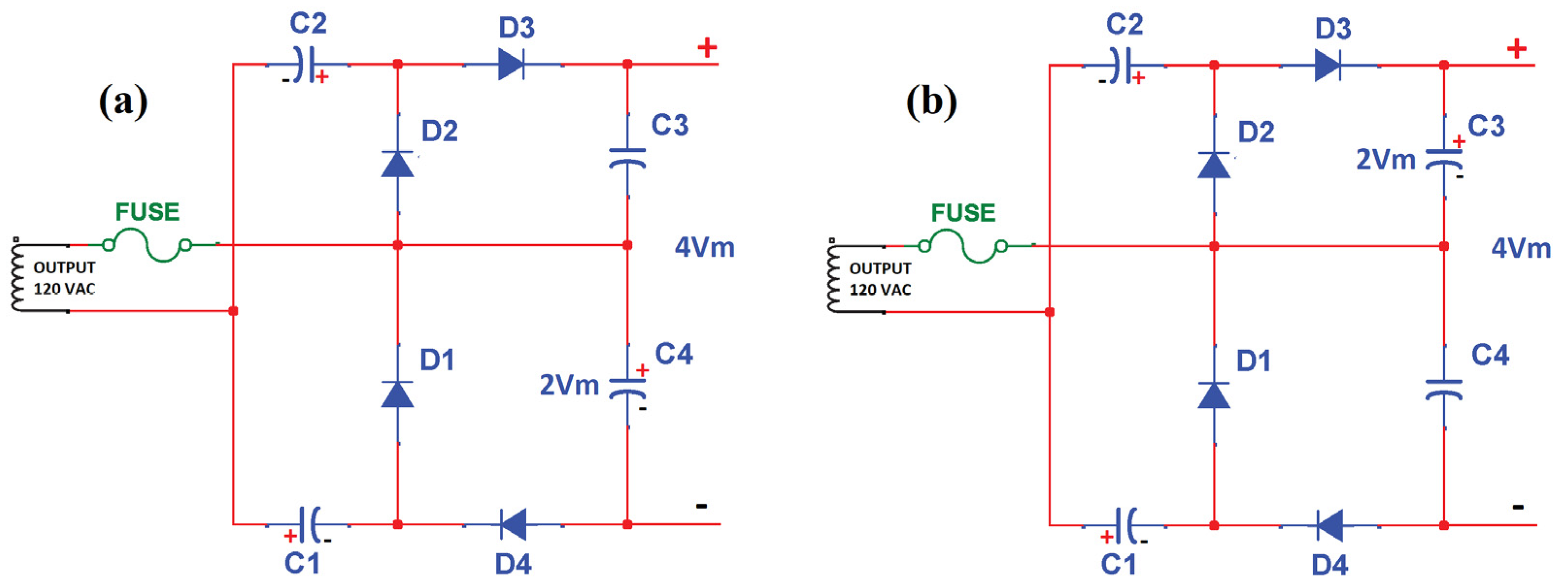
Figure 4.
High power drive circuit devices. (A) N-channel enhancement mode MOSFET, (Second) dimming circuit.
Figure 4.
High power drive circuit devices. (A) N-channel enhancement mode MOSFET, (Second) dimming circuit.

Figure 5.
Complete electronic schematic of pulsed HVDC power supply using PWM generator.
Figure 5.
Complete electronic schematic of pulsed HVDC power supply using PWM generator.

Figure 6.
Pulsed HVDC power supply prototype. (A) DC/AC inverter, (Second) voltage quadruple circuit, (C) PWM generator circuit, (d) MOSFET gate drive circuit and dimmer circuit and (e) Arduino Nanoboard.
Figure 6.
Pulsed HVDC power supply prototype. (A) DC/AC inverter, (Second) voltage quadruple circuit, (C) PWM generator circuit, (d) MOSFET gate drive circuit and dimmer circuit and (e) Arduino Nanoboard.
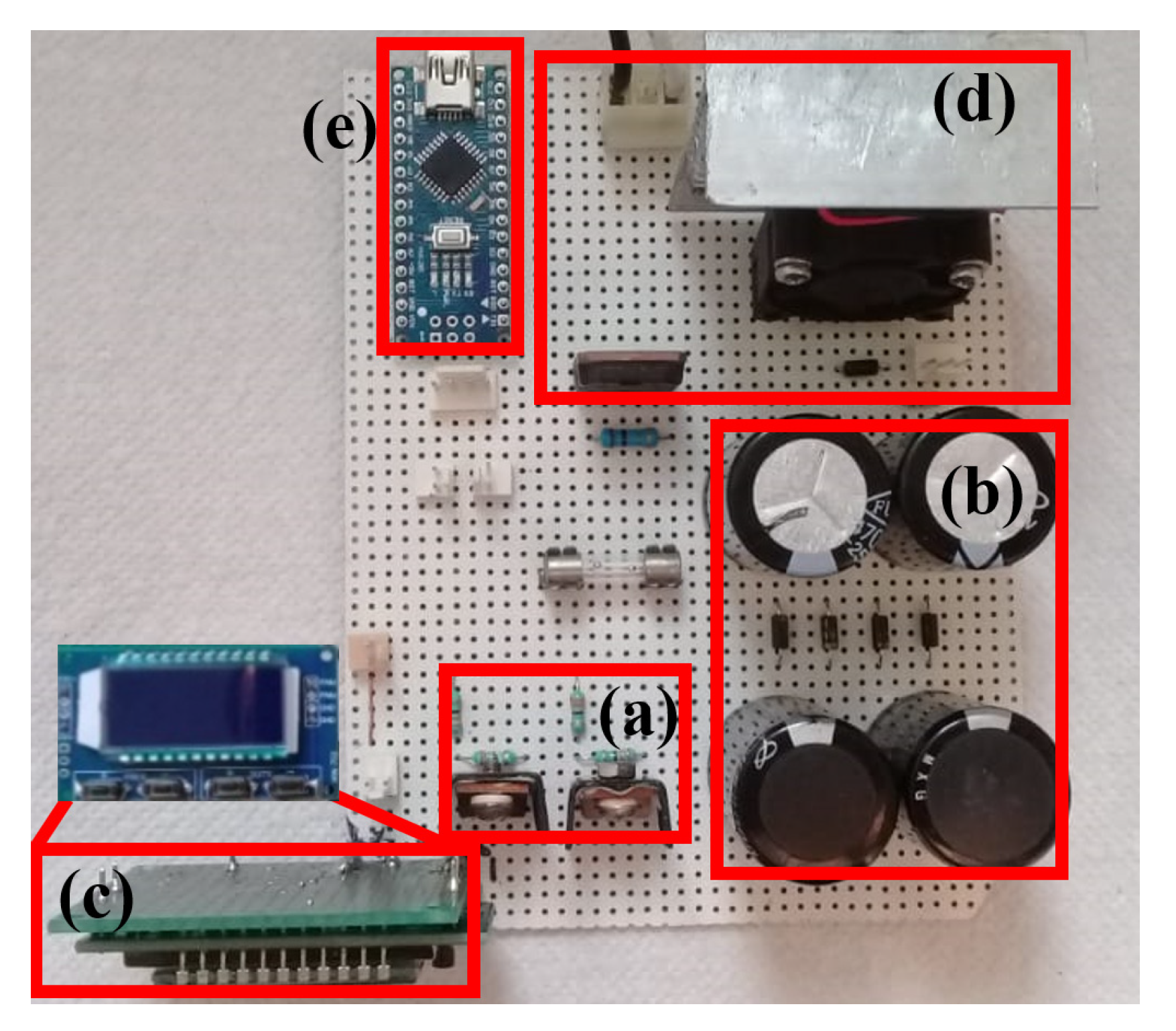
Figure 7.
experimental device. (A) TDS1001B oscilloscope, (Second) pulsed HVDC prototype and (C) A 50-watt lamp was used as the test load.
Figure 7.
experimental device. (A) TDS1001B oscilloscope, (Second) pulsed HVDC prototype and (C) A 50-watt lamp was used as the test load.
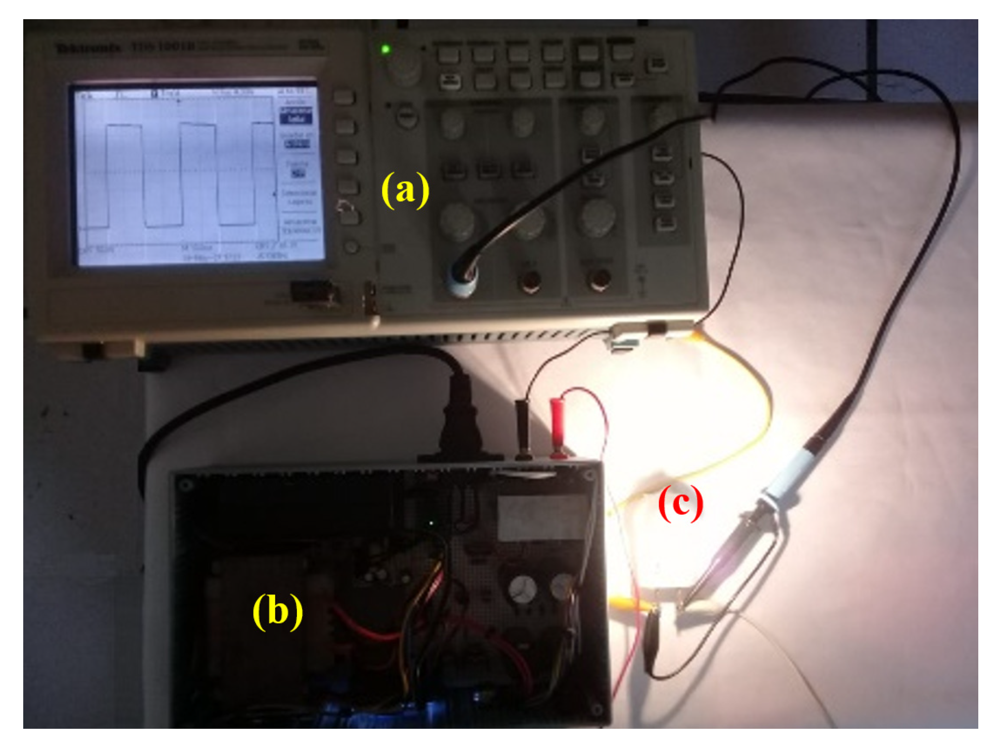
Figure 8.
(A) Glass base board,(Second) copper strip and (C) stainless steel 304.
Figure 8.
(A) Glass base board,(Second) copper strip and (C) stainless steel 304.
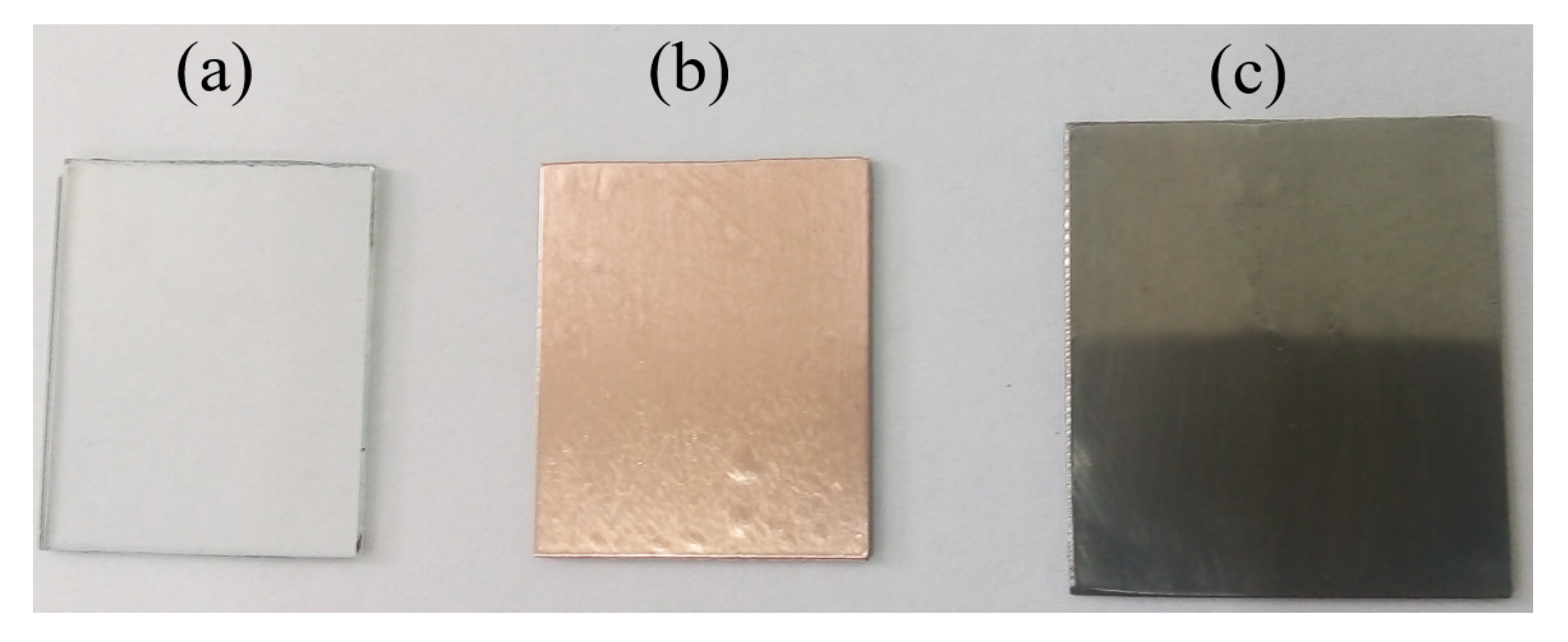
Figure 9.
Experimental setup for preparing SiC coating.
Figure 9.
Experimental setup for preparing SiC coating.
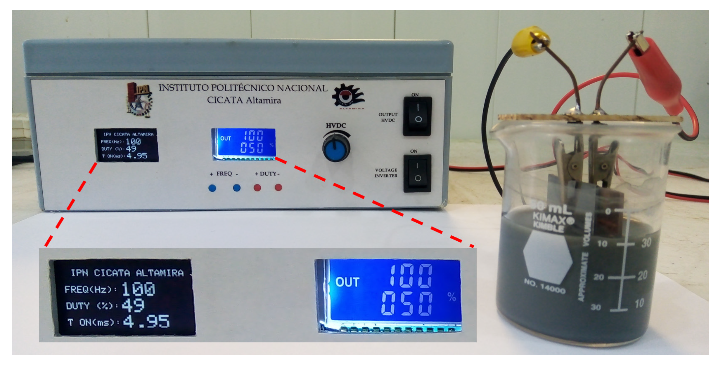
Figure 10.
(A) The copper tape is coated with SiC, (Second) SiC is compacted and heat treated at 500 °C.
Figure 10.
(A) The copper tape is coated with SiC, (Second) SiC is compacted and heat treated at 500 °C.
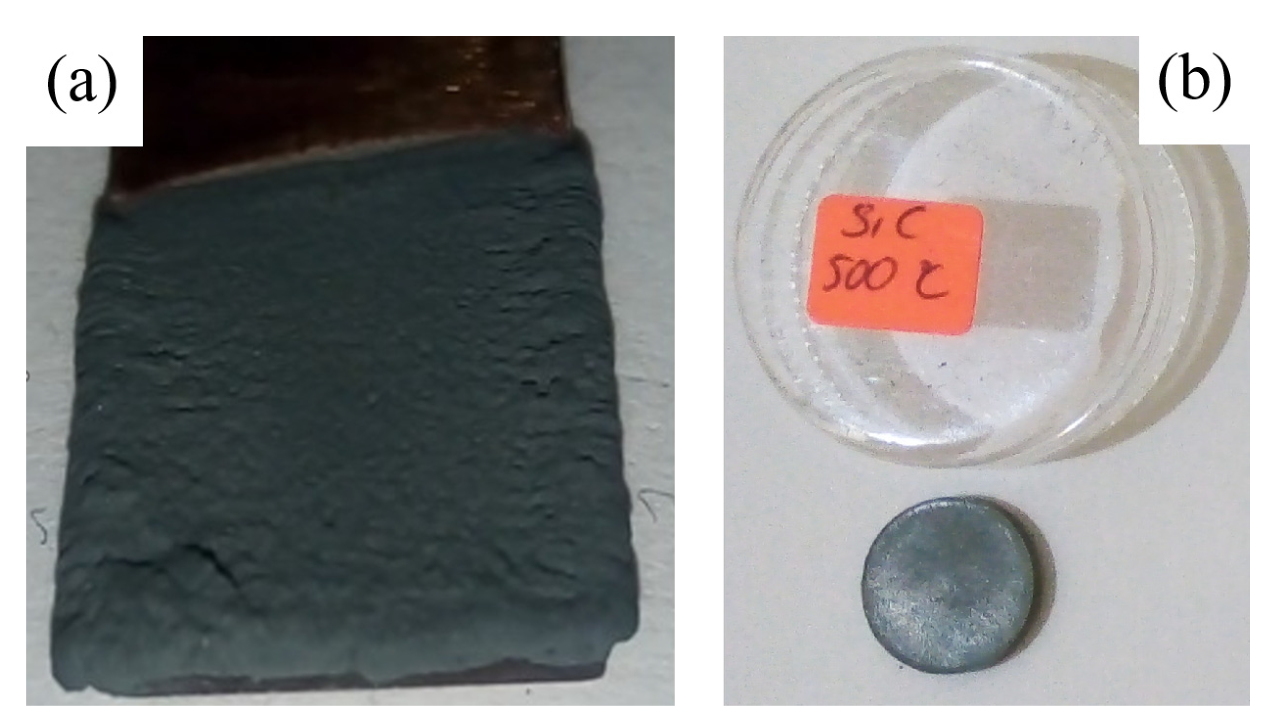
Figure 11.
Complete prototype of pulsed HVDC power supply.
Figure 11.
Complete prototype of pulsed HVDC power supply.
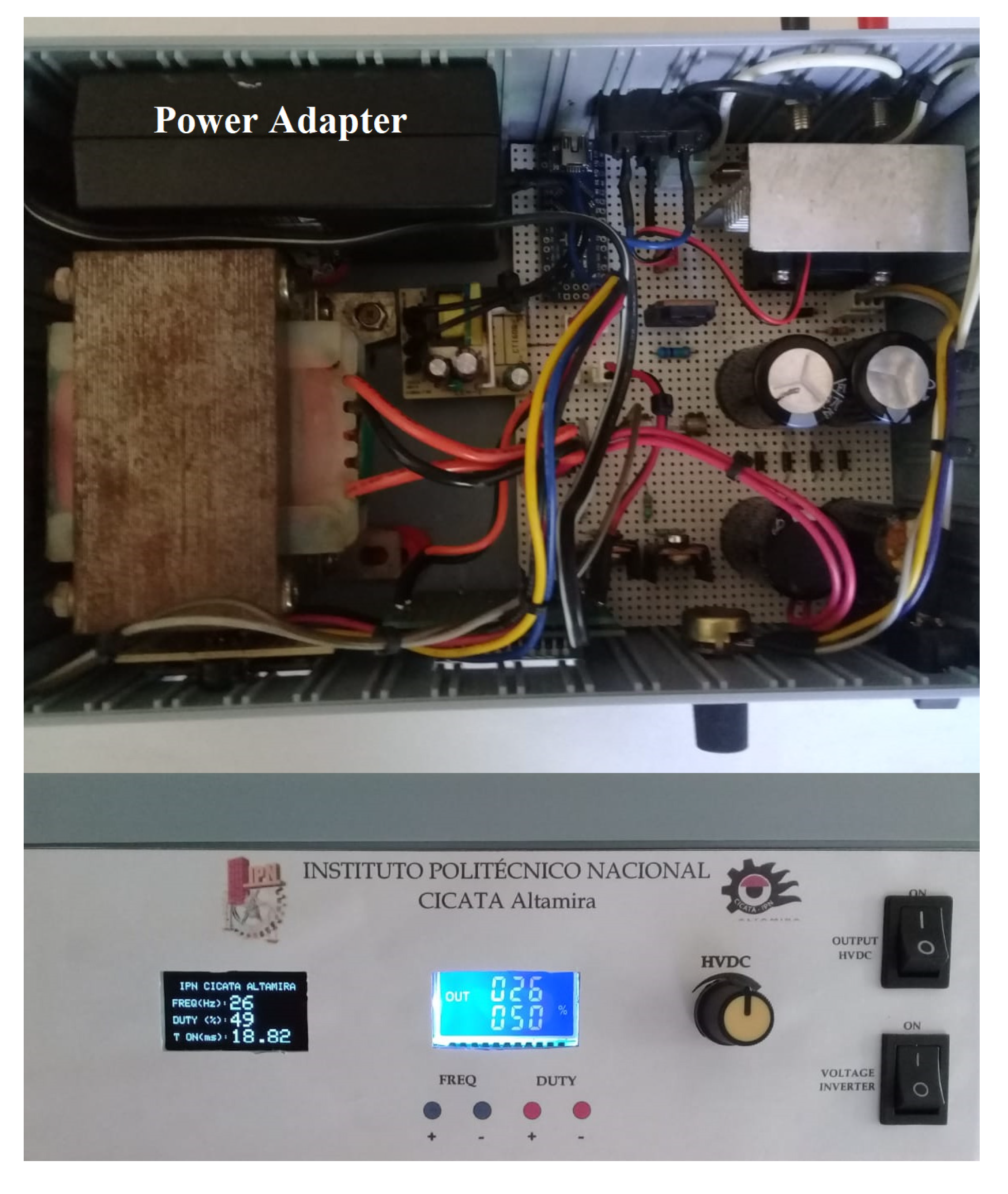
Figure 12.
The voltage signal is measured at the output of the voltage inverter under no-load conditions.
Figure 12.
The voltage signal is measured at the output of the voltage inverter under no-load conditions.
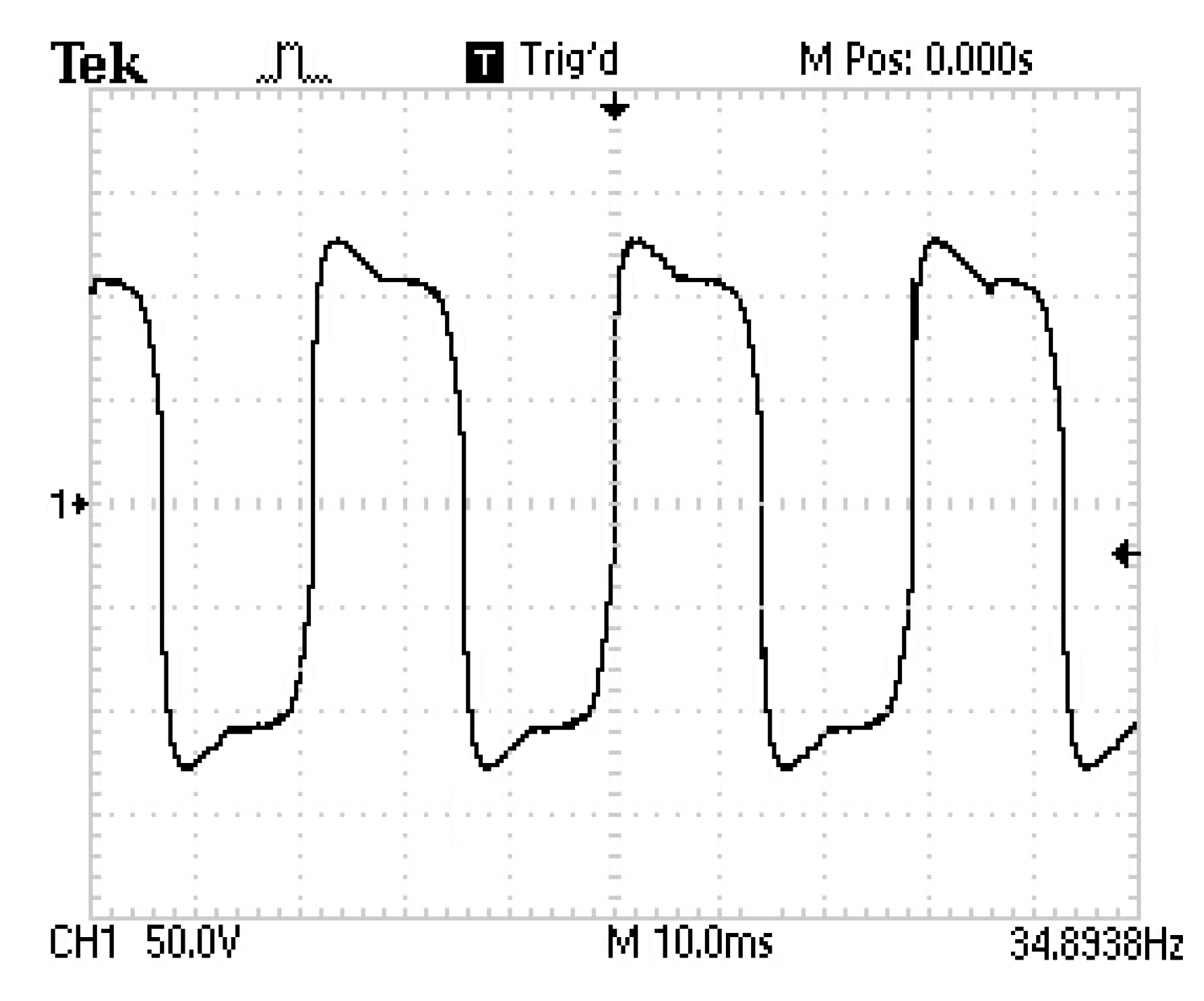
Figure 13.
The voltage signal is measured at the output of the PWM generator without load.
Figure 13.
The voltage signal is measured at the output of the PWM generator without load.
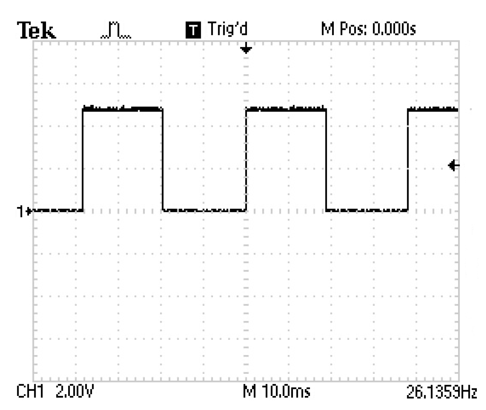
Figure 14.
Experimental PWM gating signal at no load.
Figure 14.
Experimental PWM gating signal at no load.
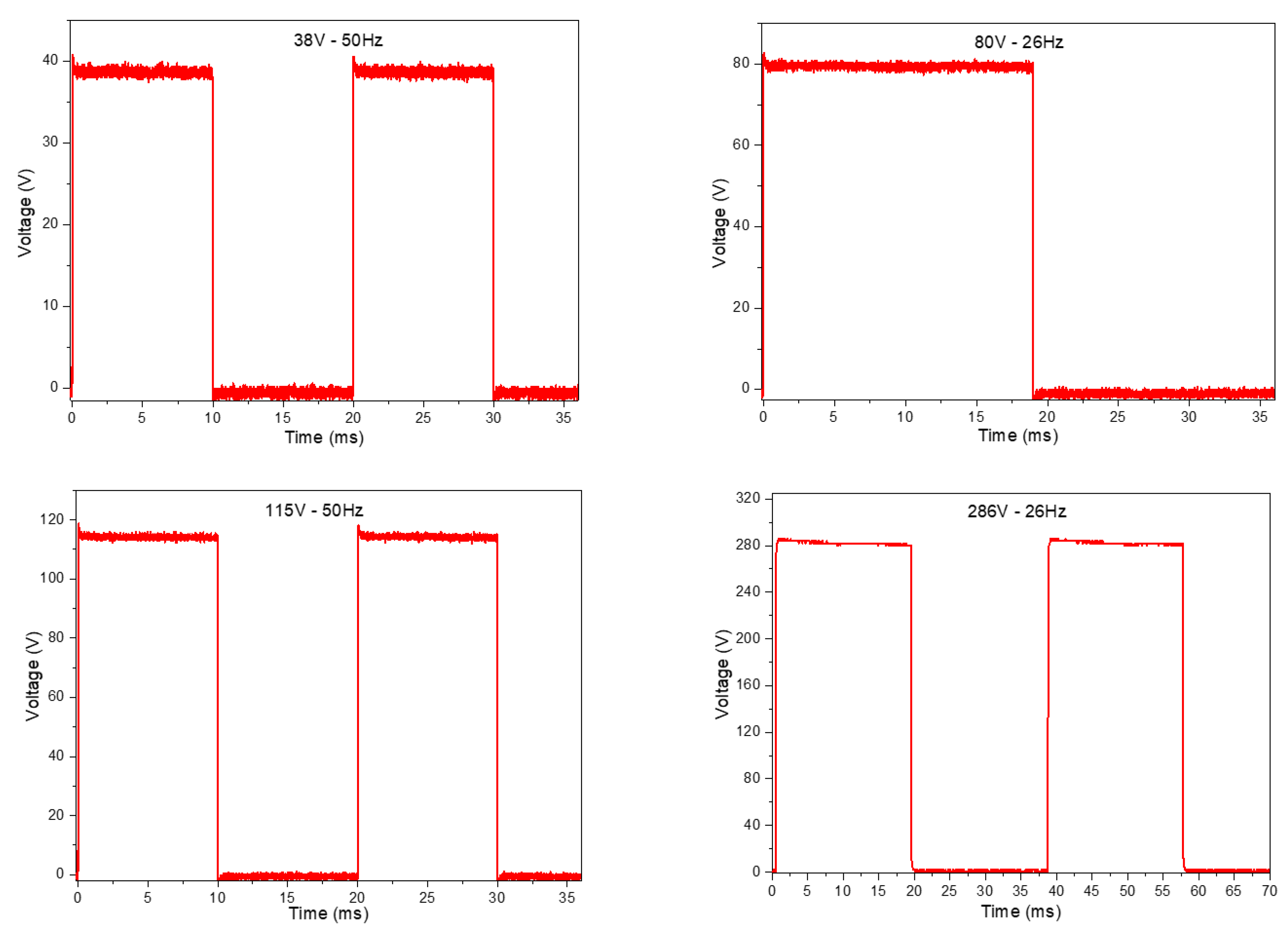
Figure 15.
X-ray diffraction patterns of SiC, alumina and graphite powders.
Figure 15.
X-ray diffraction patterns of SiC, alumina and graphite powders.
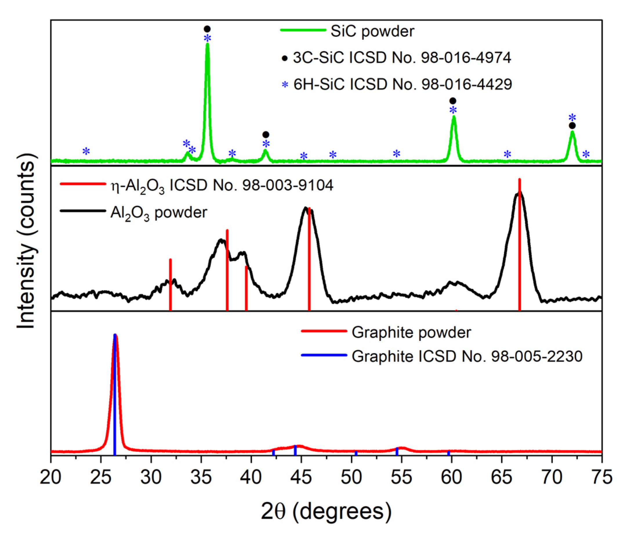
Figure 16.
Fine XRD pattern of SiC heat treated at 500 °C. Blue squares correspond to 3C SiC, green squares correspond to 6H SiC, and vertical lines relate to the crystallographic planes of each phase.
Figure 16.
Fine XRD pattern of SiC heat treated at 500 °C. Blue squares correspond to 3C SiC, green squares correspond to 6H SiC, and vertical lines relate to the crystallographic planes of each phase.
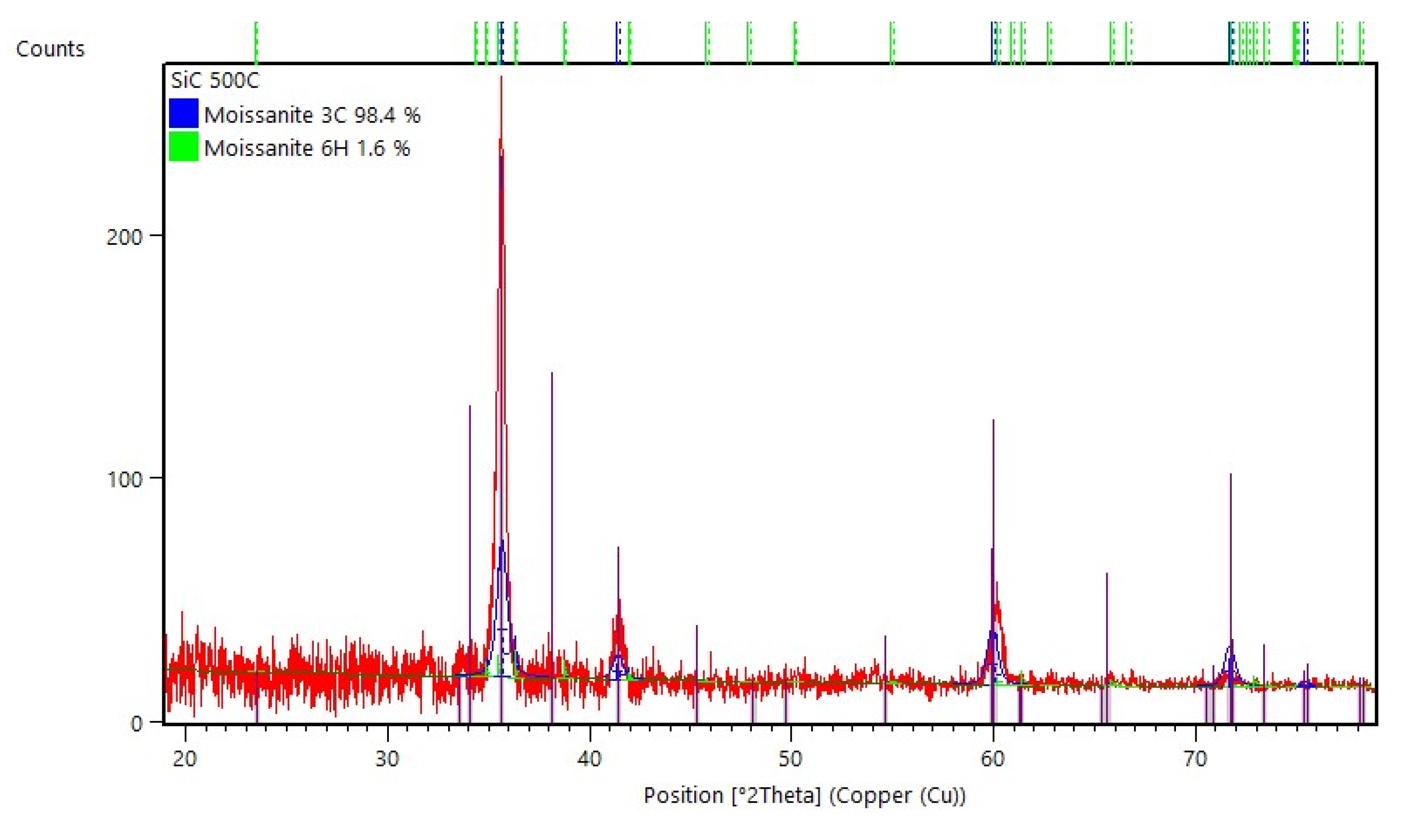
Figure 17.
X-ray diffraction of SiC samples heat treated at 500 °C and SiC mixed with alumina and/or graphite.
Figure 17.
X-ray diffraction of SiC samples heat treated at 500 °C and SiC mixed with alumina and/or graphite.
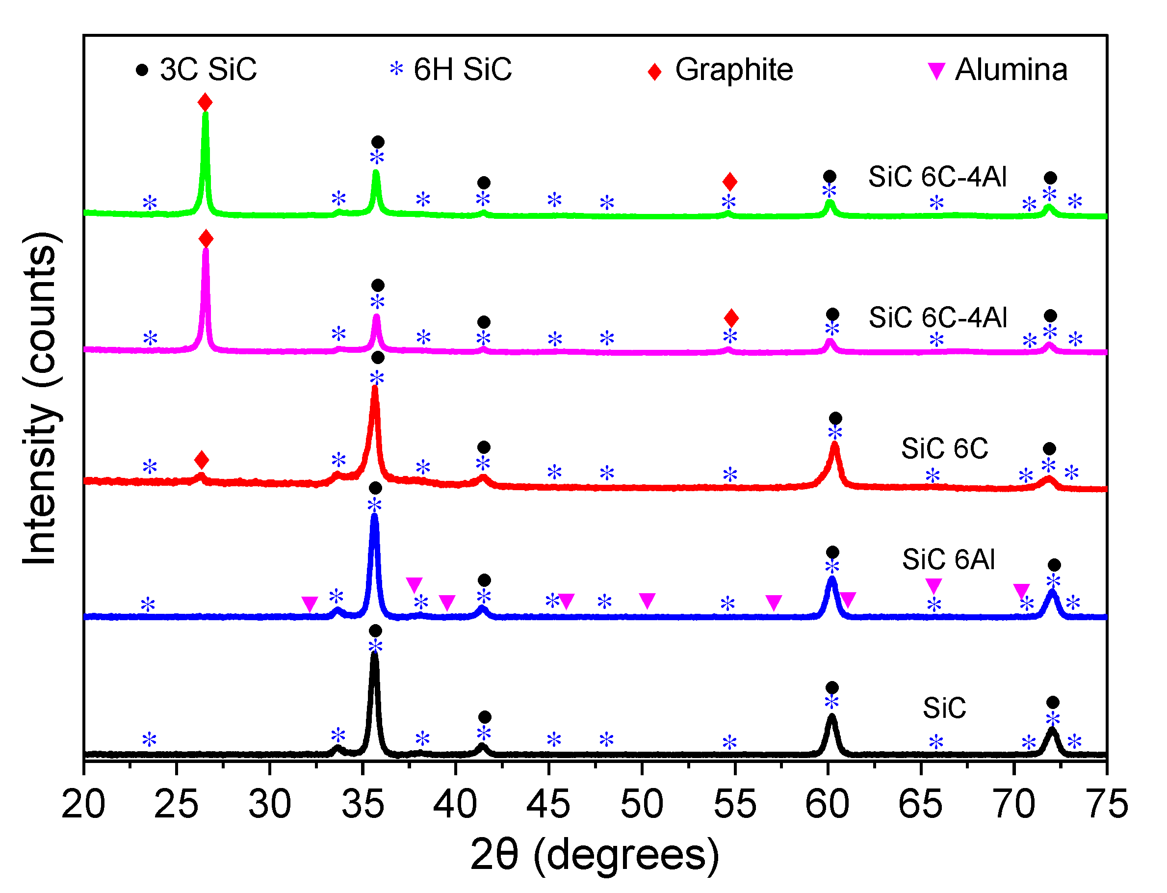
Figure 18.
Raman spectra of SiC and SiC samples mixed with alumina and/or graphite.
Figure 18.
Raman spectra of SiC and SiC samples mixed with alumina and/or graphite.
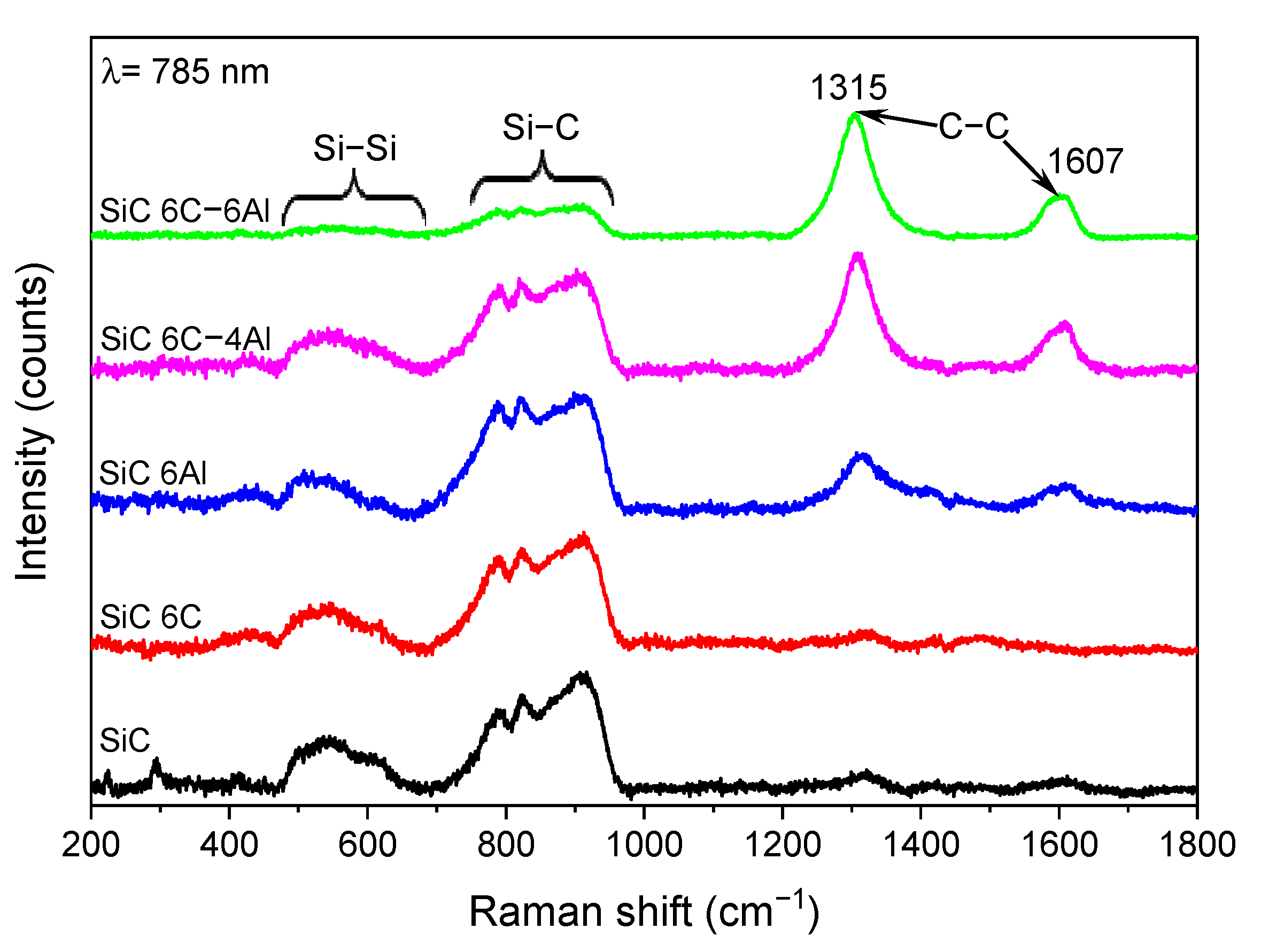
Figure 19.
Deconvoluted Raman spectra of SiC samples.
Figure 19.
Deconvoluted Raman spectra of SiC samples.
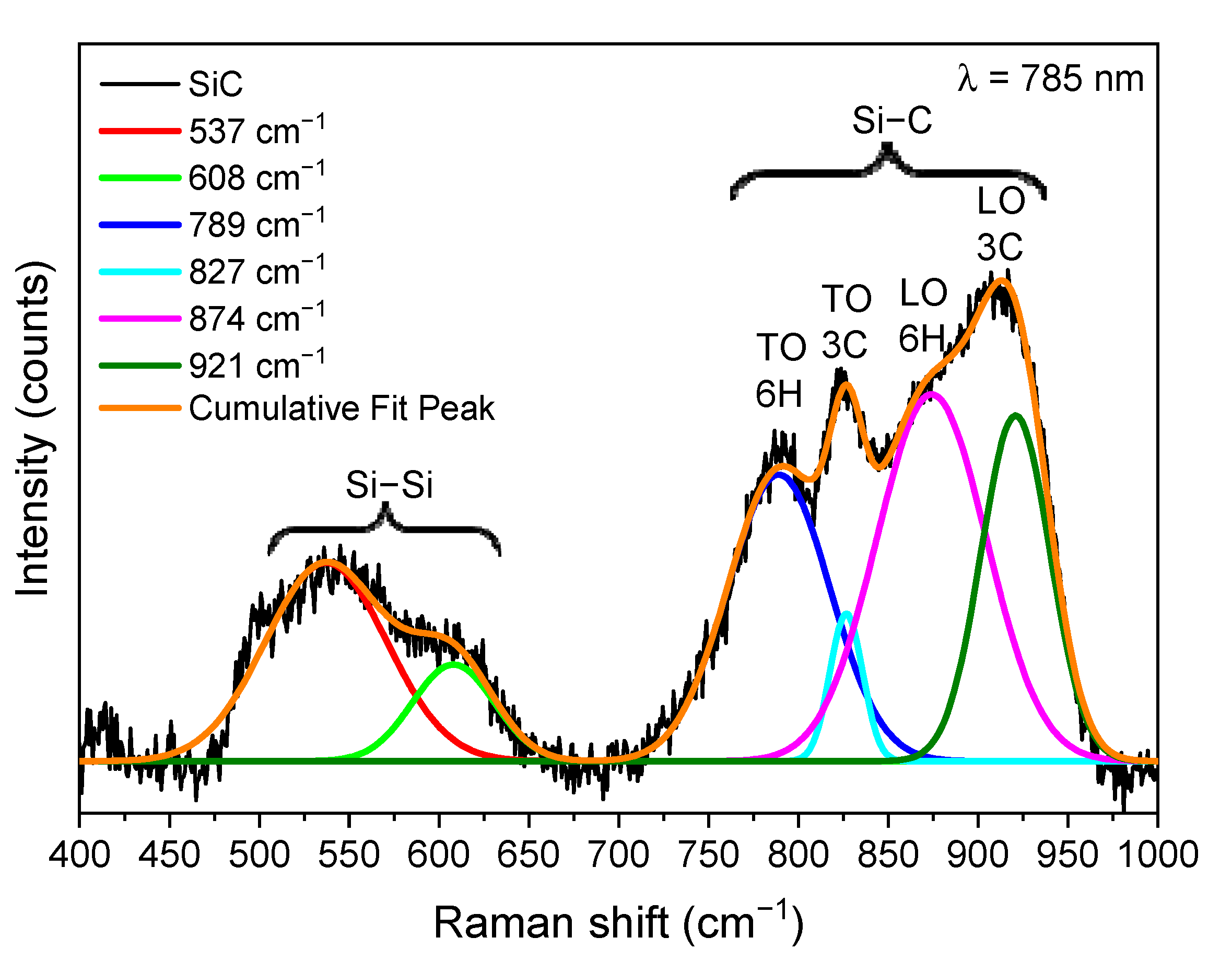
Figure 20.
SEM micrograph of compacted sample, (A) Silicon carbide 500×, (Second) silicon carbide, (C) Silicon carbide 6C, (d) Silicon carbide 6Al, (e) SiC 6C-4Al and (F) SiC 6C-6Al at 5000×, the yellow circles are graphite and the red circles are cracks.
Figure 20.
SEM micrograph of compacted sample, (A) Silicon carbide 500×, (Second) silicon carbide, (C) Silicon carbide 6C, (d) Silicon carbide 6Al, (e) SiC 6C-4Al and (F) SiC 6C-6Al at 5000×, the yellow circles are graphite and the red circles are cracks.
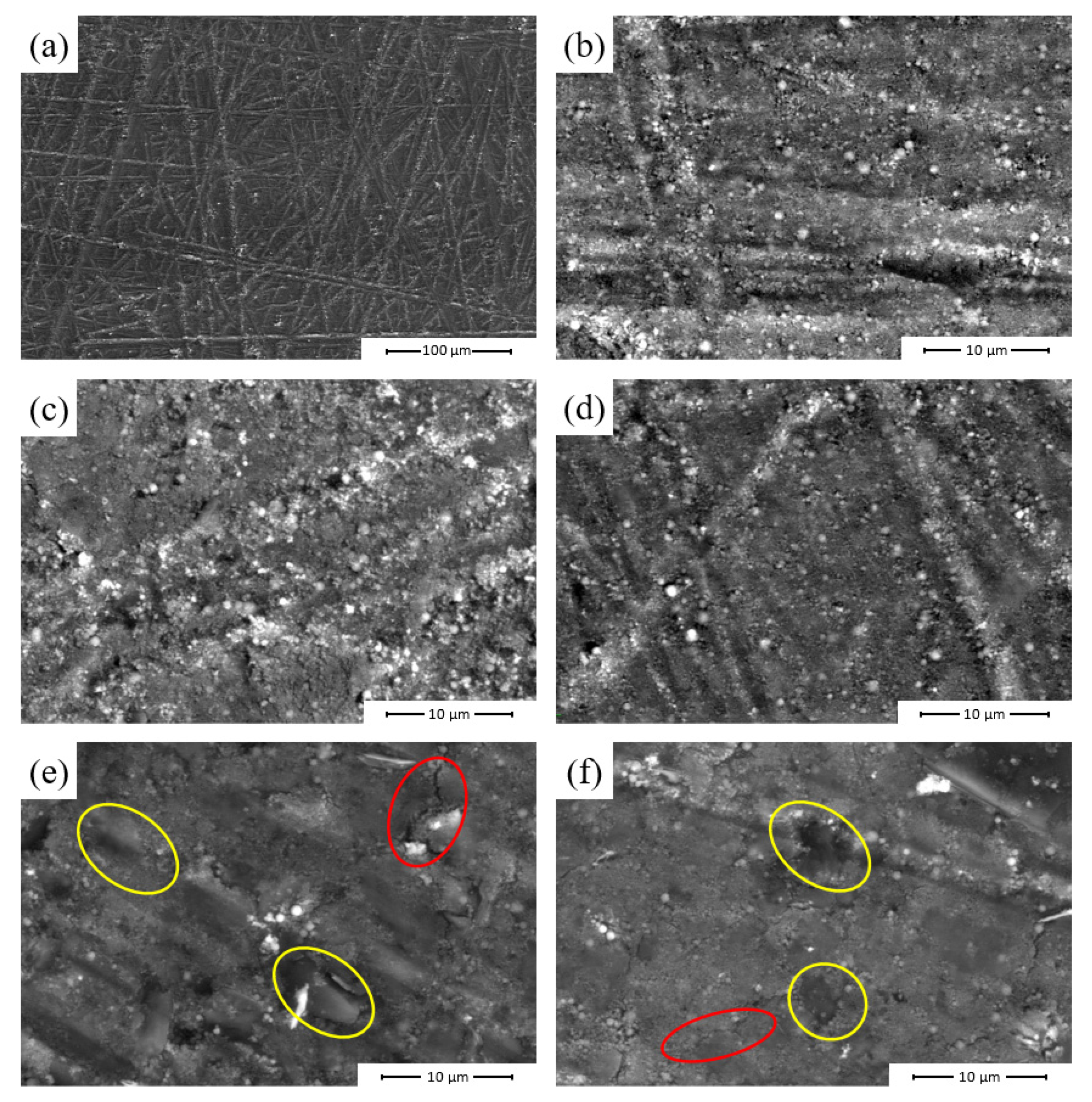
Figure 21.
Picture at the end of the electrophoretic deposition method.
Figure 21.
Picture at the end of the electrophoretic deposition method.
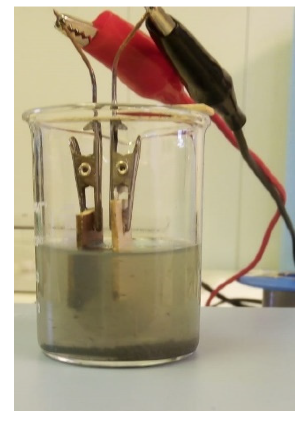
Figure 22.
Elemental composition of SiC and SiC samples mixed with alumina and/or graphite.
Figure 22.
Elemental composition of SiC and SiC samples mixed with alumina and/or graphite.

Figure 23.
Electrical conductivity of SiC and SiC mixed with alumina and/or graphite as a function of temperature.
Figure 23.
Electrical conductivity of SiC and SiC mixed with alumina and/or graphite as a function of temperature.
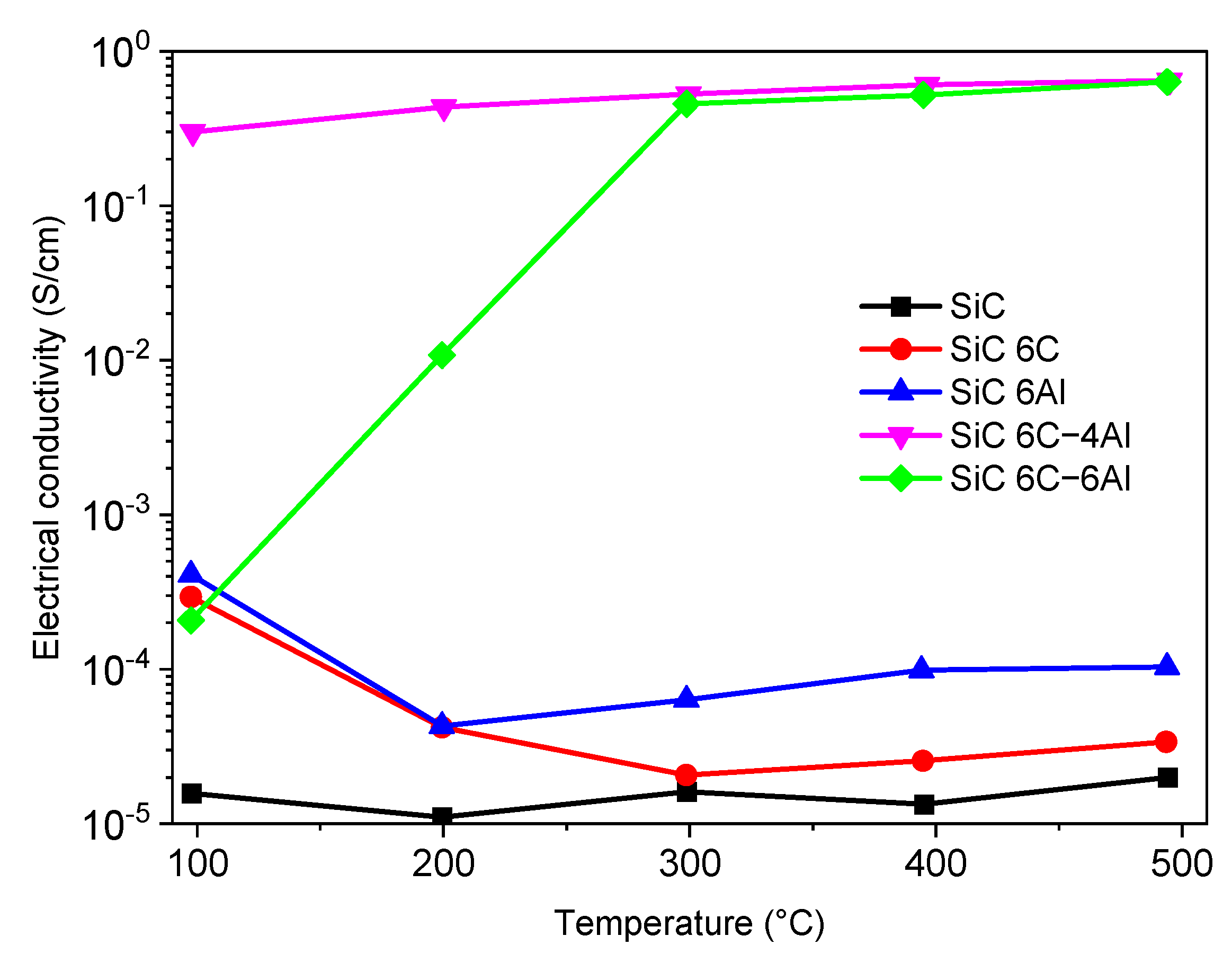
Figure 24.
Temperature dependence of the Seebeck coefficient of SiC and SiC mixed with alumina and/or graphite.
Figure 24.
Temperature dependence of the Seebeck coefficient of SiC and SiC mixed with alumina and/or graphite.
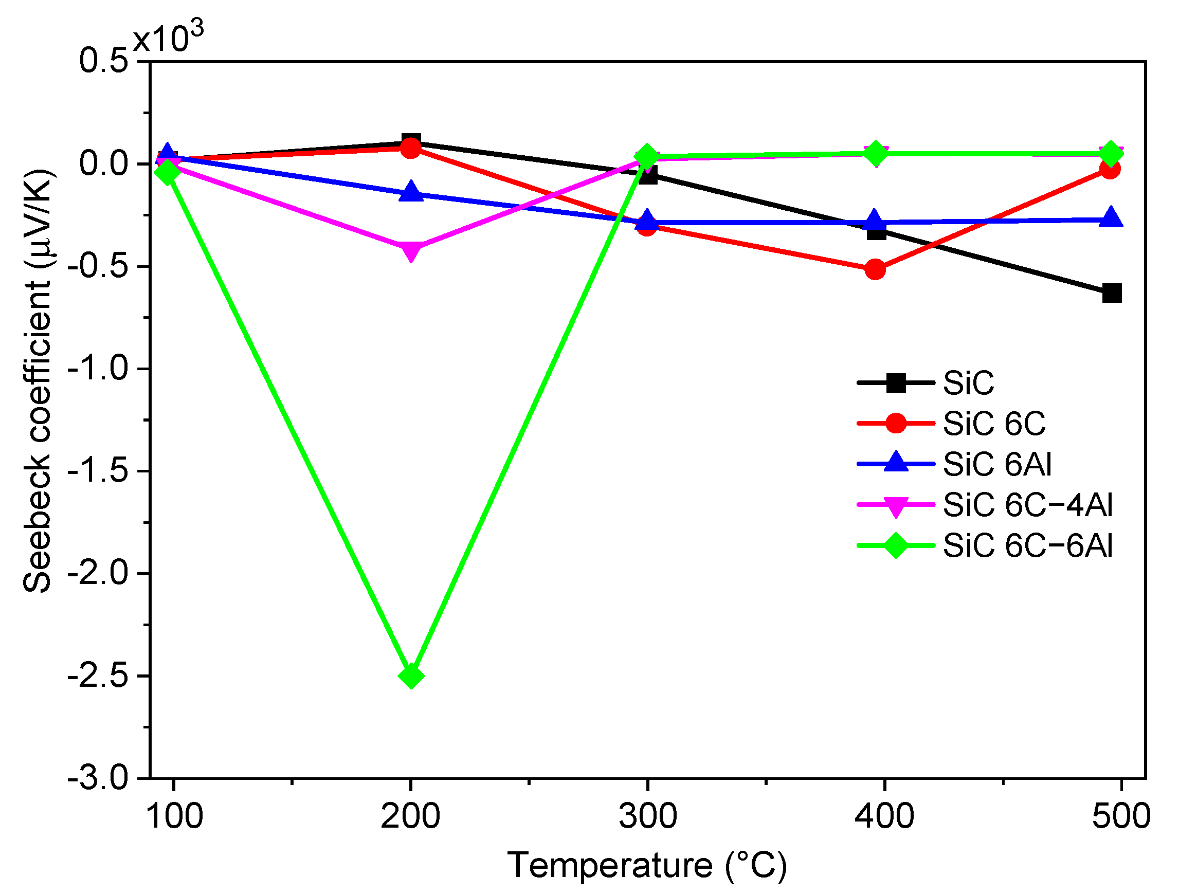
Figure 25.
Thermal conductivity of SiC and SiC mixed with alumina and/or graphite as a function of temperature.
Figure 25.
Thermal conductivity of SiC and SiC mixed with alumina and/or graphite as a function of temperature.

Figure 26.
Temperature dependence. (A) electronic thermal conductivity and (Second) Lattice thermal conductivity of SiC and SiC mixed with alumina and/or graphite.
Figure 26.
Temperature dependence. (A) electronic thermal conductivity and (Second) Lattice thermal conductivity of SiC and SiC mixed with alumina and/or graphite.
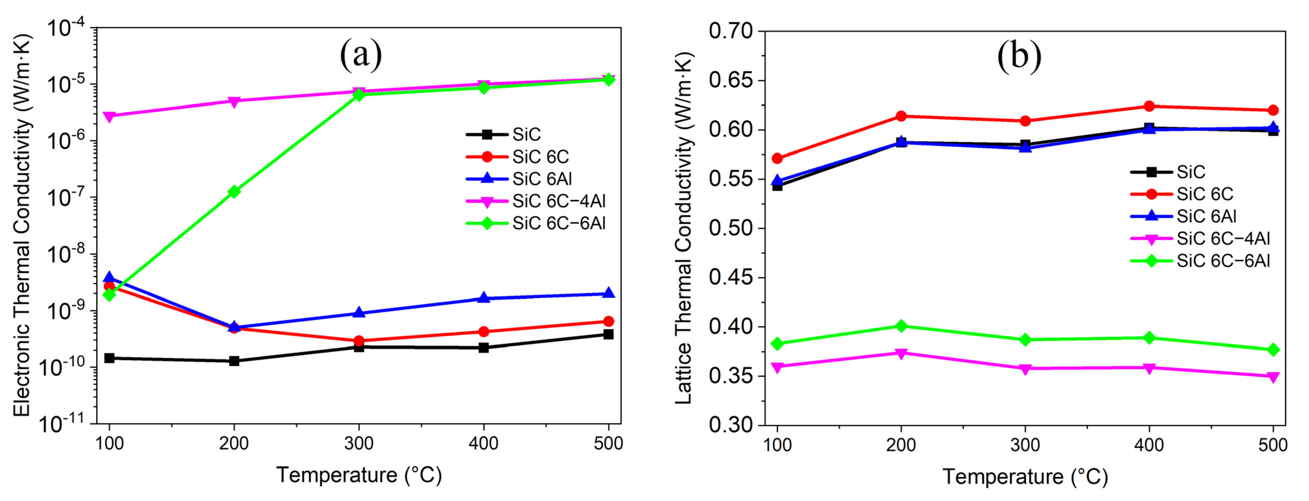
Figure 27.
The figure of merit (ZT) of SiC and SiC mixed with alumina and/or graphite changes with temperature.
Figure 27.
The figure of merit (ZT) of SiC and SiC mixed with alumina and/or graphite changes with temperature.

Table 1.
Nomenclature for SiC samples with graphite and aluminum oxide components.
Table 1.
Nomenclature for SiC samples with graphite and aluminum oxide components.
| Nomenclature example | Ingredients (% by weight) | ||
|---|---|---|---|
| silicon carbide | C | aluminum2oxygen3 | |
| silicon carbide | 100 | – | – |
| Silicon carbide 6C | 100 | 6 | – |
| Silicon carbide 6 aluminum | 100 | – | 6 |
| Silicon carbide 6C-4Al | 100 | 6 | 4 |
| Silicon carbide 6C-6Al | 100 | 6 | 6 |
Table 2.
Specifications of the pulsed HVDC prototype.
Table 2.
Specifications of the pulsed HVDC prototype.
| scope | value |
|---|---|
| Input voltage (DC) | 12 |
| Input current (A) | 1.25 |
| Output voltage (DC) | 0–430 |
| Output stable current during pulse period (mA) | 0.3–60 |
| Pulse frequency (kHz) | 0–150 |
| Cyclic load(%) | 0–100 |
table 3.
The structural and lattice parameters of SiC heat-treated at 500 °C were obtained through Rietveld refinement of XRD data.
table 3.
The structural and lattice parameters of SiC heat-treated at 500 °C were obtained through Rietveld refinement of XRD data.
| stage | weight% | H2 | rightExperience | rightp | rightwettable powder | One (angstrom) | C(O) | Volume (Å3) | r (g/cm3) |
|---|---|---|---|---|---|---|---|---|---|
| 3C silicon carbide | 98.4 | 1.18 | 20.82 | 24.32 | 22.64 | 4.37202 | 83.5694 | 3.19 | |
| 6H silicon carbide | 1.6 | 3.02414 | 15.23072 | 120.6325 | 3.31 |