JEDEC on Tuesday released the official specification for GDDR7 DRAM, the latest version of the long-standing memory standard for graphics cards and other GPU-powered devices. The latest generation of GDDR brings a combination of memory capacity and memory bandwidth gains, the latter driven primarily by switching to PAM3 signals on the memory bus. The latest graphics RAM standard also increases the number of channels per DRAM chip, adds new interface training modes, and introduces on-chip ECC to maintain efficient memory reliability.
“JESD239 GDDR7 marks a significant advancement in high-speed memory design,” said Mian Quddus, Chairman of the JEDEC Board of Directors. “With the shift to PAM3 signaling, the memory industry has a new path to extend the performance of GDDR devices and drive graphics and a variety of high-performance devices.” Continuous development of applications. “
GDDR7 has been in development for several years, with members of JEDEC first revealing the memory technology about a year ago, when Cadence revealed the use of PAM3 encoding as part of its verification tools. Since then, we’ve heard from multiple memory manufacturers that we can expect the final version of the memory to launch in 2024, with the JEDEC launch largely on schedule.
As mentioned earlier, the biggest technical change in GDDR7 is the conversion of two-bit non-return-to-zero (NRZ) encoding on the memory bus to three-bit pulse amplitude modulation (PAM3) encoding. This change allows GDDR7 to transfer 3 bits of data in two cycles, 50% more data than GDDR6 running at the same clock speed. As a result, GDDR7 can support higher overall data transfer rates, which is a key component in making each generation of GDDR successively faster than its predecessor.
| GDDR generation | |||||
| GDDR7 | GDDR6X (Non-JEDEC) |
GDDR6 | |||
| Each pin black and white | 32 Gbps (first generation) 48 Gbps (spec maximum) |
24 Gbps (transport) | 24 Gbps (sampling) | ||
| Chip density | 2GB (16GB) | 2GB (16GB) | 2GB (16GB) | ||
| Total black and white (256-bit bus) | 1024 GB/sec | 768 GB/sec | 768 GB/sec | ||
| memory voltage | 1.2V | 1.35V | 1.35V | ||
| data rate | Democratic Germany | Democratic Germany | Democratic Germany | ||
| signaling | PAM-3 | PAM-4 | NRZ (binary) | ||
| maximum density | 64GB | 32GB | 32GB | ||
| Package | 266 FBGA | 180 FBGA | 180 FBGA | ||
The first generation of GDDR7 is expected to run at data rates of around 32 Gbps per pin, and memory manufacturers have previously said that rates as high as 36 Gbps/pin are easily achievable. However, the GDDR7 standard itself leaves room for higher data rates (up to 48 Gbps/pin), with JEDEC even claiming “up to 192 GB/s” for GDDR7 memory chips [32b @ 48Gbps] It is worth noting that this is much higher than the bandwidth increase brought by the PAM3 signal itself, which means that there are multiple levels of enhancement in the design of GDDR7.
Digging deeper into the specification, JEDEC also once again subdivides a single 32-bit GDDR memory chip into a higher number of channels. GDDR6 provides two 16-bit channels, while GDDR7 extends this to four 8-bit channels. From an end-user perspective, this distinction is somewhat arbitrary – no matter what, it’s still a 32-bit chip running at 32Gbps/pin – but it has a big impact on how the chip works internally. In particular, JEDEC retains the 256-bit prefetch per channel of GDDR5 and GDDR6, making GDDR7 a 32n prefetch design.
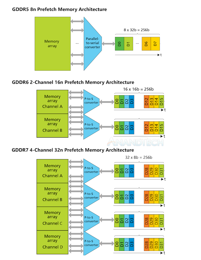
GDDR channel architecture.Original GDDR6 era chart provided by Micron
The net effect of all this is that by halving the channel width but keeping the prefetch size the same, JEDEC effectively doubles the amount of data a DRAM cell can prefetch per cycle. This is a pretty standard trick for extending DRAM memory bandwidth, and is essentially the same thing JEDEC did with GDDR6 in 2018. But it’s a reminder that DRAM cells are still very slow (on the order of hundreds of MHz) and aren’t getting any faster. Therefore, the only way to provide a faster memory bus is to fetch more and more data at once.
Changes in the number of channels per memory chip also have a smaller impact on how multi-channel “clamshell” mode works with higher-capacity memory configurations. GDDR6 accesses a single memory channel from each chip in a clamshell configuration, while GDDR7 will access two channels – JEDEC calls it dual-channel mode. Specifically, this mode reads channels A and C from each chip. It actually behaves the same way as GDDR6 clamshell mode, which means that while the latest generation of memory still supports clamshell configurations, no tricks have been used to increase memory capacity other than increasing memory chip density.
It is worth noting that the GDDR7 standard officially adds support for 64Gbit DRAM devices, which is twice the maximum capacity of GDDR6/GDDR6X of 32Gbit. It also continues to support non-quadratic capacity, supporting 24Gbit and 48Gbit chips. Support for larger memory chips further pushes the theoretical maximum memory capacity of high-end graphics cards with a 384-bit memory bus to up to 192GB of memory – a development that will no doubt be welcomed by data center operators in the era of high-capacity data centers. Language artificial intelligence model. Still, although GDDR6 supports 32Gbit chips, we still often see 16Gbit memory chips used on today’s memory cards. Coupled with the fact that Samsung and Micron have revealed that their first-generation GDDR7 chips will also reach 16Gbit/24Gbit respectively, it’s safe to say that 64Gbit chips are still far away now (so don’t sell them without using 48GB cards yet).
For the latest generation of memory technology, JEDEC also includes several new GDDR memory reliability features. Most notably, there is on-chip ECC functionality, similar to what we saw when DDR5 was launched. While we have yet to get official comment from JEDEC as to why they have chosen to include ECC support now, the inclusion of ECC support is not surprising given the reliability requirements of DDR5. Simply put, as memory chip density increases, it becomes increasingly difficult to produce “perfect” chips without defects; therefore, adding on-chip ECC allows memory manufacturers to keep their chips reliable when they encounter the inevitable errors run.
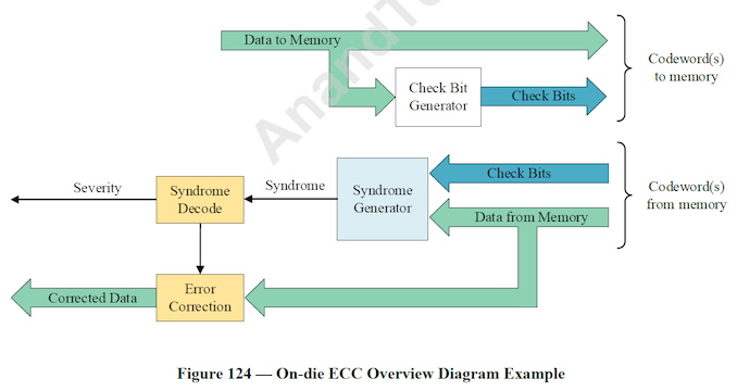
This figure is reproduced with permission from JEDEC document JESD239, Figure 124
Internally, the GDDR7 specification requires at least 16 bits of parity data (6.25%) for every 256 bits of user data, and JEDEC gives an example implementation of a 9-bit single error correction code (SEC) plus 7-bit cyclic redundancy check (CRC ). Overall, GDDR7 on-chip ECC should be able to correct 100% of 1-bit errors and detect 100% of 2-bit errors – in the rare case of 3-bit errors, the detection rate drops to 99.3%. Information about memory errors is also provided to the memory controller through what JEDEC calls the on-chip ECC transparent protocol. Although technically separate from ECC itself, GDDR7 also introduces another memory reliability feature, Command Address Parity with Command Blocking (CAPARBLK), designed to improve the integrity of the command address bus.
Otherwise, it remains to be seen what this will mean for workstation and server video cards, although the inclusion of on-chip ECC will likely have no greater impact on consumer graphics cards than it does on DDR5 memory and consumer platforms. Vendors out there have been using soft ECC on unprotected memory for several generations; presumably this is also true for GDDR7 cards, but the regular use of soft ECC makes things more flexible than in the CPU world.
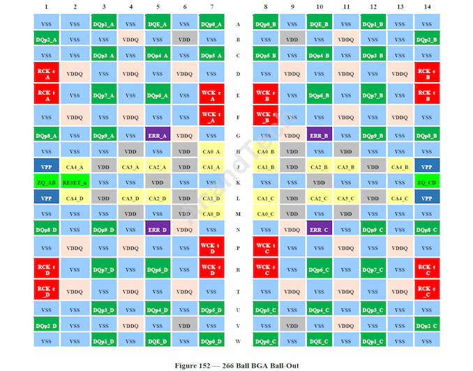
This figure is reproduced with permission from JEDEC document JESD239, Figure 152
Finally, GDDR7 also introduces a series of other reliability-related features, mainly related to aiding PAM3 operation. This includes core-independent LFSR (Linear Feedback Shift Register) training mode with eye masking and error counters. LFSR training mode is used to test and tune the interface (to ensure efficiency), eye masking evaluates signal quality, and error counters track the number of errors during training.
Technical issues aside, this week’s announcements also included statements of support from all the major players on both sides of the aisle, including AMD and NVIDA, as well as the trio of Micron/Samsung/SKhynix. It goes without saying that given the memory capacity and bandwidth improvements brought by GDDR7, all parties are keen to use or sell GDDR7 respectively, especially in this era when any product targeting the AI market is a hot seller.
No specific products have been announced yet, but since Samsung and Micron have previously announced their intention to launch GDDR7 memory this year, we should see the new memory (and new GPUs paired with it) later this year.
JEDEC standards and publications are copyrighted by the JEDEC Solid-State Technology Association. all rights reserved.